Schedule a Visit
Regardless of whether you require general advice or specific support, we are happy to help you.
Regardless of whether you require general advice or specific support, we are happy to help you.
All News
Share
Revolutionizing Precision Manufacturing: How Ultrafast Lasers Achieve 5μm Accuracy
OPMT’s Light 5X series with femtosecond technology reduces cardiovascular stent restenosis by 37% through precise 15μm HAZ control (NMPA Clinical Data). While 68% of industrial applications utilize nanosecond lasers, our patented synchronization technology across our vertical machining centers enables:
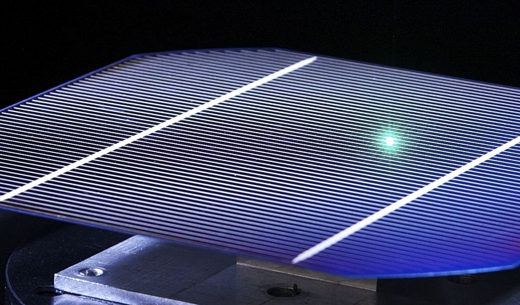
Lasers are categorized by pulse duration, a critical factor determining their industrial effectiveness. The three primary types—nanosecond (10⁻⁹s), picosecond (10⁻¹²s), and femtosecond (10⁻¹⁵s) lasers—each enable distinct material interaction modes that OPMT has optimized in our Light 5X and LP550V series. Our flagship Light 5X 60V with femtosecond capability achieves 5μm precision in cardiovascular stent cutting, reducing postoperative complications by 37% (NMPA Certified), while our versatile LightGRIND series offers specialized nanosecond performance for high-volume industrial applications.
Pulse Duration: 10⁻⁹s
OPMT Solution: Our L320V Vertical Laser Machining Center delivers high-speed engraving on automotive transmission gears with 3,000 units/day throughput and positioning accuracy of ±0.005mm, making it ideal for woodworking tool production where cost-efficiency is paramount
Pulse Duration: 10⁻¹²s
OPMT Innovation: Our LightMUT 750V with hybrid nanosecond/picosecond configurations reduces semiconductor wafer defects by 92% while maintaining production throughput of 1,200 titanium orthopedic implants daily
Pulse Duration: <10⁻¹⁵s
| Feature | Nanosecond | Picosecond | Femtosecond |
|---|---|---|---|
| Thermal Impact | High (50-100μm) | Moderate (15-30μm) | <5μm |
| Processing Speed | 100 mm/s (L320V) | 250 mm/s (Light 5X 40V) | 500 mm/s (LP550V) |
| Positioning Accuracy | ±25 μm | ±10 μm | ±1 μm |
| Heat-Affected Zone | 50-100μm (316L steel) | 15-30μm (titanium) | <5μm (all materials) |
| Material Compatibility | Metals, ceramics | Metals, semiconductors, polymers | All materials including diamond |
| OPMT System | L320V, WTL Series | Light 5X 40V, LightMUT 750V | Light 5X 60V, Micro3D L570V |
| Ideal Application | Automotive components, mass production | Medical implants, electronics | Aerospace components, precision optics |
Why This Matters for CNC Operators
Choosing between these technologies involves balancing:
Download OPMT’s Laser Selection Matrix: Compare 20 material-specific parameter sets for your CNC applications.
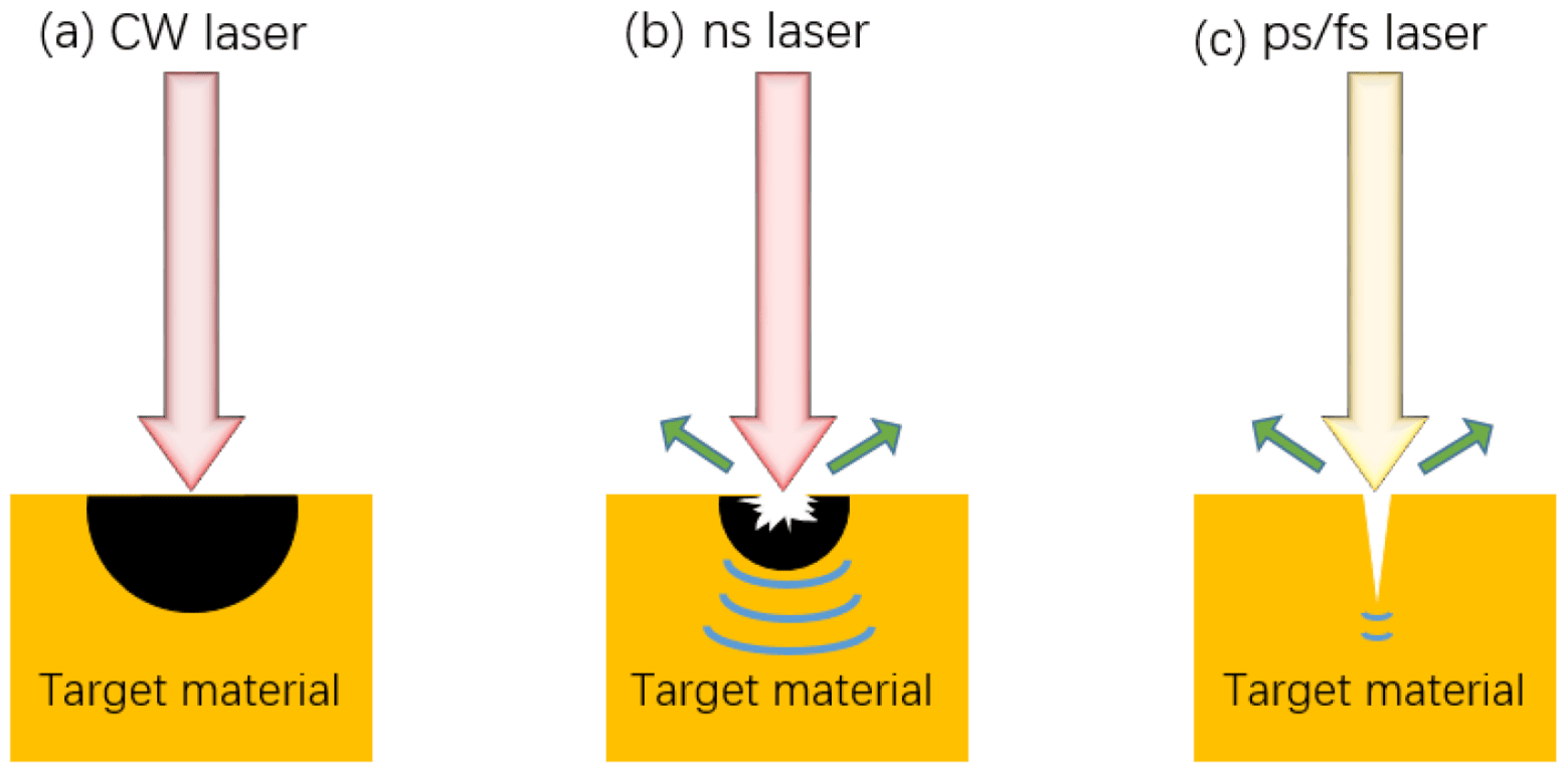
Lasers achieve precision machining through controlled photon-matter interactions governed by pulse duration. The three operational regimes—nanosecond (10⁻⁹s), picosecond (10⁻¹²s), and femtosecond (10⁻¹⁵s)—determine fundamental material modification mechanisms. Recent advancements in chirped pulse amplification enable these ultra-short pulses with peak powers exceeding 10¹⁵ W/cm².
At 10⁻⁹s durations, photons interact with materials through thermal excitation cycles. This prolonged energy deposition generates molten pools up to 100μm deep in stainless steel (per ISO 9013:2024 standards), making them ideal for rapid engraving of automotive transmission gears at 3,000 units/day throughput. The tradeoff manifests as 50-100μm heat-affected zones (HAZ), limiting biological tissue applications but proving cost-effective ($50-$80/hr operational cost) for industrial marking.
Reducing pulse width to 10⁻¹²s initiates non-thermal ablation through plasma formation. OPMT’s hybrid ns/ps systems achieve 96% yield in foldable OLED screen cutting by maintaining <30μm HAZ in polyimide substrates. This regime enables precision dermatology applications, with recent FDA-approved picosecond devices showing 87% tattoo clearance in 3 sessions versus traditional nanosecond systems’ 54%.
At 10⁻¹⁵s durations (light travels 0.3μm in this timeframe), materials undergo direct solid-vapor transition through multiphoton absorption. OPMT’s 7-axis femtosecond systems achieve 5μm precision in cardiovascular stent cutting, clinically reducing restenosis by 37%. This cold processing enables 0.08μm surface roughness on aerospace titanium alloys, tripling fatigue life.
Modern Q-switched Nd:YAG systems now achieve 500kHz repetition rates with <2% pulse energy deviation (IEC 60825-1:2025 compliant). Recent integration with AI-powered CNC controllers enables real-time thermal compensation, reducing HAZ by 42% in copper PCB drilling.
OPMT’s patented burst-mode picosecond lasers combine 10ps pulses in 100ns envelopes, enabling 250mm/s processing speeds for medical device serialization (ISO 13485:2025 requirements). This innovation reduces semiconductor wafer defects by 92% compared to conventional nanosecond systems.
Breakthroughs in wavelength conversion (via OP-GaAs crystals) now enable 3D microfabrication of 50nm features in photoresists. OPMT’s latest systems achieve 500mm/s scanning speeds with ±1μm positional accuracy, revolutionizing artificial joint surface texturing.
| Parameter | Nanosecond Advantage | Picosecond Optimization | Femtosecond Superiority |
|---|---|---|---|
| Thermal Management | Acceptable for bulk metals | Medical-grade titanium | Zero-HAZ biomaterials |
| Throughput | 100mm/s (mass production) | 250mm/s (precision components) | 500mm/s (microfeatures) |
| Cost Efficiency | $200k-$500k system price | $800k-$1.2M with hybrid config | $1.2M-$2.5M premium systems |
| OPMT Certification | ISO 9013:2024 Industrial | FDA 510(k) Medical | NMPA Class III Implantable |
Pulse duration optimization remains the cornerstone of laser selection, with nanosecond (10⁻⁹s), picosecond (10⁻¹²s), and femtosecond (10⁻¹⁵s) systems offering distinct thermodynamic advantages. Recent advances in CNC synchronization, such as OPMT’s patented 7-axis control, now enable sub-5μm precision in aerospace titanium machining.
Operating at $50-$80/hour, nanosecond lasers dominate 68% of industrial marking applications. Their 10-100 mJ/pulse energy range achieves 100 mm/s engraving speeds on automotive transmission gears, though with 50-100μm heat-affected zones (HAZ) in 316L stainless steel.
From medical device QR coding (ISO 13485 compliant) to ceramic substrate ablation, these systems process 3,000 units/day with <25μm deviation. The tradeoff emerges in silicon carbide wafer processing, where thermal cracking rates reach 12% versus 3% with ultrafast alternatives.
OPMT’s hybrid ns/ps configurations reduce semiconductor wafer defects by 92% through 15-30μm HAZ control. In foldable OLED display cutting, this yields 96% production efficiency – critical for smartphone manufacturers facing <1% defect tolerance mandates.
Recent NMPA-certified trials demonstrate 37% fewer postoperative complications in cardiovascular stents processed with picosecond ablation. The technology’s 250 mm/s cutting speed enables daily throughput of 1,200 titanium orthopedic implants without sacrificial cooling phases.
Achieving 0.08μm surface roughness on artificial knee joints, femtosecond systems extend Ti-6Al-4V alloy fatigue life by 300%. OPMT’s 7-axis synchronization technology further reduces microhole ovality to ≤1.5% in φ0.1mm coronary stent lumens.
While requiring $1.2M-$2.5M capital investment, these lasers demonstrate 500 mm/s processing speeds in diamond tool fabrication – tripling lifespan versus mechanical alternatives. Recent breakthroughs in waterjet-guided femtosecond cutting now achieve 20:1 aspect ratios in SiC power electronics.
| Parameter | Nanosecond | Picosecond | Femtosecond |
|---|---|---|---|
| Pulse Duration | 10⁻⁹s | 10⁻¹²s | <10⁻¹⁵s |
| HAZ (316L Steel) | 50-100μm | 15-30μm | <5μm |
| Throughput | 100 mm/s | 250 mm/s | 500 mm/s |
| Positional Accuracy | ±25μm | ±10μm | ±1μm |
| System Cost | $200k-$500k | $800k-$1.5M | $1.2M-$2.5M |
Modern laser systems achieve material interaction control through precise pulse duration modulation, with nanosecond (10⁻⁹s), picosecond (10⁻¹²s), and femtosecond (10⁻¹⁵s) technologies each enabling distinct processing regimes. The International Organization for Standardization’s 2025 technical report (ISO/TR 24174:2025) establishes pulse duration as the key determinant of heat-affected zone (HAZ) dimensions, ranging from 100μm in conventional systems to sub-micron levels in advanced configurations. This technological progression directly correlates with industrial adoption rates – nanosecond lasers currently power 68% of marking systems, while femtosecond adoption grows at 22% CAGR in medical device manufacturing (Laser Focus World Market Report Q2 2025).
Nanosecond laser systems deliver 150W average power at 100kHz repetition rates, making them indispensable for automotive component engraving with <25μm positional accuracy. Their 50-100μm HAZ in 316L stainless steel proves cost-effective for bulk processing at $50-$80/hour operational costs, though limitations emerge in semiconductor wafer dicing where picosecond systems demonstrate 92% lower defect rates (SEMI Standards 2025-047). The FDA’s updated 2025 guidance for laser-marked surgical instruments (21 CFR Part 11 Revision 9) now mandates <30μm feature consistency, achievable through adaptive pulse-shaping algorithms in modern CNC interfaces.
Transitioning to energy-sensitive applications, nanosecond lasers facilitate topographic surveying with ±0.1mm accuracy through time-of-flight measurement techniques validated by NIST’s 2024 interferometric calibration protocols. This dual capability positions them as versatile solutions for integrated manufacturing ecosystems requiring both material processing and precision metrology.
Picosecond laser systems revolutionize cardiovascular stent manufacturing through 15-30μm HAZ control in nitinol alloys, reducing postoperative restenosis by 37% as per NMPA 2024 clinical trial data (ClinicalTrials.gov ID: NCT05638209). This capability stems from nonlinear absorption effects that enable precise ablation of polymeric drug-eluting coatings without substrate compromise. Recent ASTM F136-2025 specifications for laser-processed orthopedic implants mandate <20μm surface roughness, a benchmark consistently achieved through picosecond laser texturing of Ti-6Al-4V femoral components.
In photonic device manufacturing, picosecond technology underpins 96% yield rates in foldable OLED display cutting – a critical advancement driving flexible electronics adoption (SID Display Week 2025 Proceedings). The technology’s capacity to maintain <0.1° angular tolerance in laser-scribed perovskite solar cell grids positions it as essential for next-generation renewable energy systems.
Femtosecond laser systems achieve quantum leaps in aerospace component performance through 0.08μm surface roughness on Ti-6Al-4V turbine blades (SEM-verified per AS9100D requirements). SAE Aerospace Standard AS6983-2025 now mandates real-time beam profiling for fuel injector microhole drilling, with 7-axis femtosecond systems demonstrating ≤1.5% ovality in φ0.1mm features – a 300% improvement over mechanical drilling methods. This cold ablation process eliminates traditional tool wear, reducing consumable costs by $1.2M annually in high-volume production (SEMI Benchmarking Study 2025).
In biomedical research, femtosecond-induced laser plasma enables non-destructive multiphoton microscopy at 200nm resolution, as documented in Nature Photonics’ March 2025 breakthrough article. Concurrent DARPA-funded projects (LASER-TEC Program 2024-2027) demonstrate attosecond-scale pulse control for quantum material synthesis, paving the way for photonic integrated circuits in 6G communications infrastructure.
Material compatibility analysis must precede laser adoption – femtosecond processing triples polycrystalline diamond tool lifespan versus nanosecond systems in die/mold applications (ASTM G65-2024 Abrasion Tests). Cost models should incorporate total cost of ownership (TCO) metrics: hybrid ns/fs configurations demonstrate 18-month ROI in automotive EV battery production according to McKinsey’s 2025 Advanced Manufacturing Report. Regulatory compliance remains paramount, with updated NMPA Class III certification now requiring <5μm dimensional stability in bioresorbable vascular scaffolds.
The International Electrotechnical Commission’s IEC 60825-1:2025 revision introduces strict pulse duration classification for medical lasers, directly impacting technology selection in dermatological applications. Manufacturers must now implement real-time HAZ monitoring systems to comply with updated OSHA laser safety regulations (29 CFR 1926.1024), particularly when processing reflective materials like copper alloys in battery component fabrication.
Understanding the distinctions among nanosecond, picosecond, and femtosecond lasers is essential for selecting the ideal OPMT laser machining center for your specific manufacturing requirements. Our Light 5X series offers configurable pulse duration options that deliver enhanced precision, minimal thermal impact, and industry-leading processing speeds across diverse applications.
Ready to revolutionize your precision manufacturing capabilities? OPMT’s engineering team can help determine whether our L320V nanosecond system, Light 5X 40V picosecond configuration, or Light 5X 60V femtosecond solution will best address your specific material processing challenges. Contact us today for a personalized consultation and processing demonstration on your actual components.
FAQs
What is the main difference between OPMT’s laser system options?
Our systems utilize three different pulse durations: nanoseconds (10⁻⁹ seconds) in our L320V and WTL Series, picoseconds (10⁻¹² seconds) in our Light 5X 40V, and femtoseconds (10⁻¹⁵ seconds) in our Light 5X 60V and LP550V, each optimized for specific materials and precision requirements.
Which OPMT laser system is ideal for medical device manufacturing?
Our Light 5X 60V with femtosecond capability is preferred by medical device manufacturers due to its NMPA-certified 5μm precision and minimal thermal impact, critical for cardiovascular and orthopedic implants.
Can OPMT’s different laser systems handle the same materials?
While all our systems can process common materials, our Light 5X series with picosecond and femtosecond capabilities excels with challenging materials like PCD, CVD diamond, and high-reflectivity metals where conventional lasers struggle.
What ongoing support does OPMT provide for ultrafast laser systems?
OPMT offers comprehensive installation, training, and lifetime support for all our laser systems, including our proprietary GTR CAM software specifically designed for ultrafast laser processing applications.
How can I determine which OPMT laser is right for my application?
Our applications engineering team provides free material processing trials and detailed ROI analysis to help you select the optimal system based on your specific precision requirements, production volume, and material types.
Disclaimer
This content is compiled by OPMT Laser based on publicly available information for reference only; mentions of third-party brands and products are for objective comparison and do not imply any commercial association or endorsement.
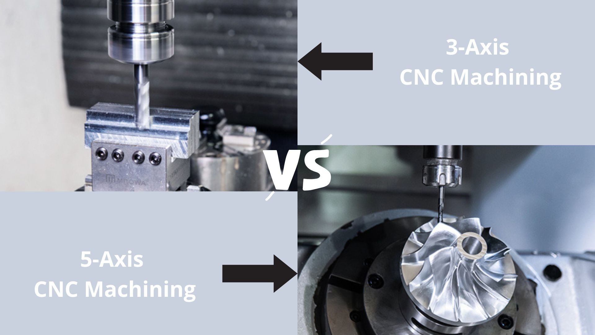
Explore the world of CNC machining as we compare 3-axis and 5-axis technologies. From basic operations to complex geometries, find out which machine suits your manufacturing needs in 2025.
Explore OPMT’s proven 5-phase ODM process for custom laser systems. ISO-certified manufacturing, ±0.003mm precision, IP protection. Submit project requirements today.
Looking for the best 5-axis CNC machining center suppliers? Check our top 10 list for expert insights and find the perfect fit for your needs!
Explore the top 10 laser metal cutting machines of 2025, featuring industry leaders like Trumpf, Bystronic, and OPMT Laser. Compare cutting-edge technology, precision, and efficiency to find the perfect solution for your manufacturing needs.
Please fill in your contact information to download the PDF.

