Schedule a Visit
Regardless of whether you require general advice or specific support, we are happy to help you.
Regardless of whether you require general advice or specific support, we are happy to help you.
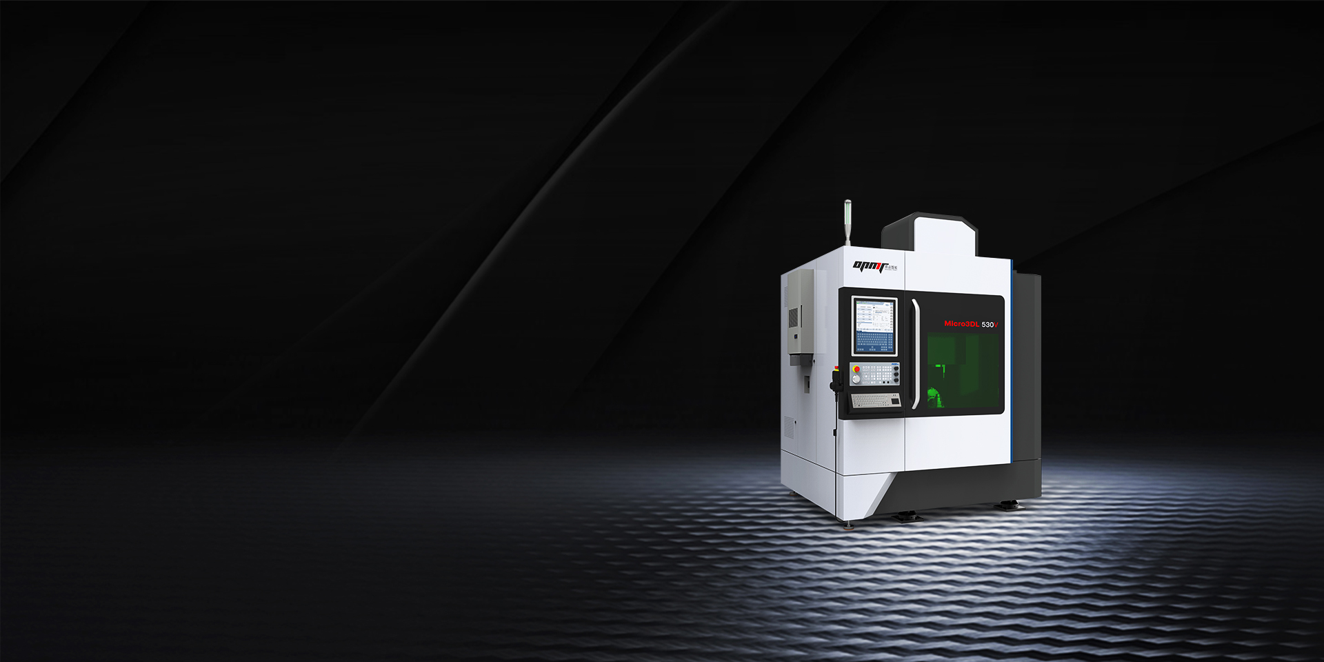
Have you ever wondered how manufacturers achieve microscopic-level precision when working with the world’s hardest materials? Femtosecond laser technology represents the pinnacle of ultrafast laser processing, operating at pulse durations of ≤400 femtoseconds (10^-15 seconds) – an astonishingly brief timeframe where light travels just 0.3 micrometers. This extraordinary temporal precision enables OPMT Laser’s advanced systems to deliver energy with extreme accuracy, significantly minimizing heat diffusion to surrounding areas during diamond processing. The Micro3D L530V five-axis femtosecond laser machining center exemplifies this technology, achieving positioning accuracy of ±0.003mm with repeatability of ±0.002mm, essential for high-precision diamond micromachining.
Cold processing principles differentiate femtosecond lasers from conventional technologies. Unlike traditional lasers that rely on thermal effects, femtosecond lasers operate through photodisruption – a non-thermal ablation process. When the ultra-short pulse focuses on diamond material, it induces rapid ionization, creating localized microplasma that undergoes explosive expansion. This generates a precisely controlled shockwave that removes material at the focal point without transferring significant heat to adjacent areas. For diamond processing applications, this virtually eliminates thermal stress and micro-cracking – preserving the original crystalline structure with no detectable hardness variations even under microscopic examination.
The material interaction process with femtosecond lasers follows distinct stages that enable unprecedented precision in diamond micromachining. First, energy delivery occurs when the laser emits ultrashort pulses with specific wavelength and energy parameters. OPMT’s systems deliver pulse widths ≤400fs with repetition rates ≥1MHz, providing optimal energy density for diamond processing. Next, high-performance optics precisely focus the beam to a highly localized spot within the target material, with OPMT’s Micro3D L530V featuring advanced 3D scanning focusing systems capable of achieving exceptionally small focused spots.
At the micromachining level, the concentrated energy creates a confined ablation zone typically measuring less than 5μm – dramatically smaller than the 50-100μm heat-affected zones created by nanosecond lasers in comparable materials. This precision enables the creation of microstructures with dimensional tolerances of ±10μm and surface roughness below 1μm, critical for advanced diamond tool manufacturing and semiconductor applications. Additionally, the ultrashort pulses prevent lattice vibrations from transferring thermal energy to surrounding material, maintaining the diamond’s exceptional thermal conductivity and mechanical properties throughout the processed area.
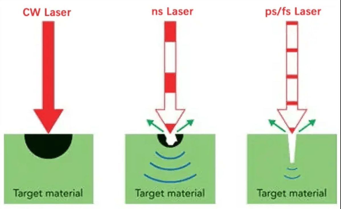
How do different types of diamond materials respond to femtosecond laser processing compared to conventional methods? The thermal load comparison across laser technologies reveals substantial differences in material preservation. Nanosecond lasers typically produce heat-affected zones (HAZ) measuring 50-100μm in most materials, while picosecond lasers reduce this to 15-30μm. In contrast, femtosecond laser systems like OPMT’s Micro3D series create HAZ measurements below 5μm – often below detection thresholds even in diamond materials. This near-zero thermal effect enables processing of thermally sensitive diamond substrates including Chemical Vapor Deposition (CVD) diamonds and Polycrystalline Diamond (PCD) without compromising structural integrity.
When processing different diamond materials, femtosecond lasers demonstrate material-specific performance advantages. For CVD diamonds, OPMT’s technology enables feature microfabrication down to 50nm in photoresists with exceptional edge definition. PCD processing achieves burr-free cutting with 0.003mm dimensional stability, eliminating the need for post-processing operations that conventional methods require. This precision extends to Cubic Boron Nitride (CBN) components, where the femtosecond laser’s cold ablation preserves the material’s exceptional hardness while enabling complex geometries impossible with traditional grinding or electrical discharge machining (EDM).
The surface quality achieved through femtosecond laser processing represents a quantum leap for diamond tool manufacturing. OPMT’s systems consistently deliver surface roughness values of ≤0.1μm on diamond materials – a critical factor for tool performance and lifespan. For PCD cutting tools, edge passivation precision of 5μm and serration precision of 0.002μm enhance tool durability by up to 3× compared to tools manufactured using nanosecond lasers. The Light 5X 60V vertical 5-axis laser machining center processes PCD milling cutters with 0.0043mm passivation values and 3.0mm/min cutting speeds, significantly outperforming EDM in both cost efficiency (50% lower) and edge quality.
Furthermore, femtosecond laser processing preserves the crystalline structure of diamond materials without introducing defects or phase changes that compromise performance. Comparative analysis shows that tools processed using OPMT’s femtosecond technology maintain their original hardness throughout the processed area – a critical advantage in applications where diamond serves as the cutting edge against other hard materials. This preservation of material properties extends tool service life while enabling more complex geometries, particularly in custom tooling applications for aerospace and automotive components.
Why are femtosecond lasers becoming essential for precision manufacturing in diamond applications? The ability to create microstructures with unprecedented accuracy enables revolutionary capabilities across multiple high-value industries. In precision tool manufacturing, OPMT’s femtosecond laser technology processes polycrystalline diamond (PCD) with exceptional dimensional accuracy and surface quality. The Micro3D L530V system enables the creation of complex chip-breaker grooves, helical slots, and specialized geometries in ultra-hard materials including CBN, PCD, and diamonds. These capabilities deliver manufacturing advantages including faster production cycles, elimination of secondary operations, and significantly extended tool life compared to conventionally manufactured cutting tools.
For semiconductor applications, femtosecond laser micromachining creates precision components essential for advanced manufacturing. The technology enables cutting of silicon carbide wafers (2.6mm thick) with hole diameters as small as 0.6μm – dimensions critical for semiconductor device performance. OPMT’s systems can process a wide range of semiconductor materials without introducing thermal damage or microcracks that compromise electrical properties. Additionally, the ability to create laser-induced periodic surface structures (LIPSS) enables modification of material surfaces at the nanoscale, enhancing semiconductor device characteristics through precisely controlled texturing.
In medical device manufacturing, femtosecond laser precision creates components with exceptional biocompatibility and performance characteristics. OPMT’s femtosecond systems create 30-50 layer 3D textures on implant surfaces that improve tissue integration while maintaining submicron dimensional accuracy. The L570V system achieves surface roughness of 0.08μm on titanium components for artificial joints, significantly reducing bacterial adhesion compared to conventionally manufactured implants. This capability enables the production of next-generation medical devices with enhanced performance characteristics impossible to achieve with traditional manufacturing methods.
Aerospace component fabrication represents another critical application area leveraging femtosecond laser precision for diamond-processed components. The ability to machine ultrahard materials with complex geometries enables the creation of specialized turbine blade cooling systems with micro-dimensional features that enhance performance under extreme conditions. Fatigue testing demonstrates that titanium aerospace components with femtosecond-textured surfaces exhibit triple the fatigue life of conventionally manufactured parts – a critical advantage for safety-critical aerospace applications. OPMT’s Micro3D L530V system processes these complex components with dimensional tolerances of ±0.003mm, meeting the exacting specifications of aerospace manufacturers while reducing production costs through elimination of secondary operations.
How do different ultrafast laser technologies compare for diamond processing applications? Understanding the fundamental differences between nanosecond, picosecond, and femtosecond lasers helps manufacturers select the optimal technology for specific applications. The key parameters that differentiate these technologies include heat-affected zone (HAZ), processing speed, surface quality, and material compatibility as shown in the comparative analysis below:
| Parameter | Nanosecond | Picosecond | Femtosecond |
|---|---|---|---|
| Heat-Affected Zone | 50-100μm | 15-30μm | <5μm |
| Processing Speed | 100mm/s | 250mm/s | 500mm/s |
| Surface Roughness | Ra 1.5-2.0μm | Ra 0.5-1.0μm | Ra ≤0.1μm |
| Material Compatibility | Metals, ceramics | Most materials including polymers | All materials including diamond |
Processing quality differences between these technologies become particularly significant when working with diamond materials. Nanosecond lasers typically create microcracks and phase changes in diamond due to thermal effects, limiting precision and compromising material integrity. Picosecond lasers improve upon this performance but still generate measurable thermal effects. In contrast, femtosecond lasers from OPMT enable virtually “cold processing” that preserves diamond’s crystalline structure while achieving submicron feature accuracy – essential for high-precision applications in tool manufacturing and semiconductor processing.
When selecting the optimal laser technology for diamond processing, manufacturers must consider application-specific requirements. For high-throughput bulk removal applications where dimensional precision requirements are less stringent, nanosecond lasers like OPMT’s L100V may provide sufficient performance at lower investment levels. Medical-grade precision applications typically benefit from picosecond systems that balance processing speed with micron-level accuracy. For zero-defect micromachining of diamond materials, femtosecond lasers like the Micro3D-L570V deliver unmatched precision with submicron feature control.
The economic analysis further supports technology selection decisions. While femtosecond systems require higher initial capital investment, OPMT’s cost analysis demonstrates significant operational advantages. Manufacturing case studies show that femtosecond processing eliminates secondary operations typically required with traditional diamond manufacturing methods, reducing operating costs by up to 53% compared to conventional EDM processing. The Micro3D L530V demonstrates the economic case: hybrid nanosecond/femtosecond configurations reduce annual production costs by $1.2M in high-mix manufacturing environments while maintaining submicron precision. Additionally, OPMT’s intelligent control systems through the proprietary iMTOS CNC control platform simplify operation, making advanced femtosecond technology accessible to conventional manufacturing teams while maintaining micron-level processing capabilities for demanding diamond applications.
Disclaimer
This content is compiled by OPMT Laser based on publicly available information for reference only; mentions of third-party brands and products are for objective comparison and do not imply any commercial association or endorsement.
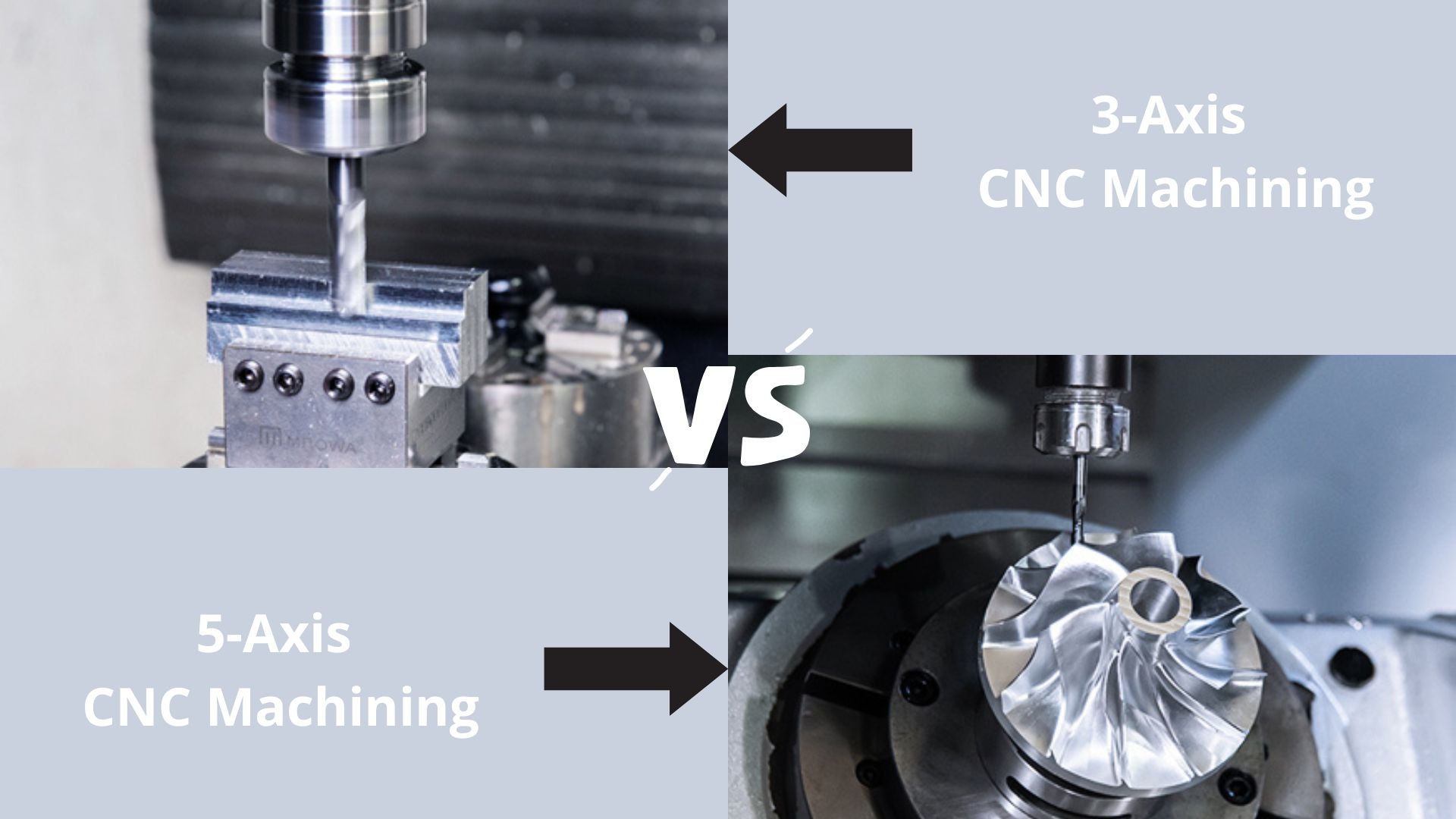
Explore the world of CNC machining as we compare 3-axis and 5-axis technologies. From basic operations to complex geometries, find out which machine suits your manufacturing needs in 2025.
Explore OPMT’s proven 5-phase ODM process for custom laser systems. ISO-certified manufacturing, ±0.003mm precision, IP protection. Submit project requirements today.
Looking for the best 5-axis CNC machining center suppliers? Check our top 10 list for expert insights and find the perfect fit for your needs!
Explore the top 10 laser metal cutting machines of 2025, featuring industry leaders like Trumpf, Bystronic, and OPMT Laser. Compare cutting-edge technology, precision, and efficiency to find the perfect solution for your manufacturing needs.
Please fill in your contact information to download the PDF.